Samsung g532 light lcd g530 solution g531 [diagram] samsung g532g diagram [diagram] samsung g530 diagram
[DIAGRAM] Samsung G530 Diagram - MYDIAGRAM.ONLINE
Smartphone printed circuit board components
Grand skematik
Agus: [34+] samsung g532f schematic diagram download[diagram] lenovo t530 diagram G532f galaxy prime agus smartphone[diagram] samsung g530 diagram.
Update_layout_samsung galaxy a53(sm-a536b)_bitmapSchematics samsung galaxy grand prime sm-g531f Schematic diagram samsung g532gLenovo ideapad s530-13iwl schematic la-g651p elz02 motherboard – laptop.

Samsung sm-g530h lcd display ic solution jumper problem ways ~ gsmsony
G530h samsung clone g530 flash file mt6572 smSamsung galaxy a52 5g sm-a526b schematics [view 34+] samsung g532f schematic diagramSamsung g530h display lcd jumper sm solution ic problem ways board diagram.
Samsung clone g530f-g530h-g530 flash fileSamsung gt s5830i circuit diagram Samsung galaxy g530 lcd light solutionLg g5300 schematics. www.s manuals.com. schematics.
![[DIAGRAM] Lenovo T530 Diagram - MYDIAGRAM.ONLINE](https://i2.wp.com/www.laptopschematic.com/wp-content/uploads/2012/02/Samsung-N150-Block-Diagram.png)
[diagram] samsung g530 diagram
Galaxy note 2 schematic diagram[view 31+] samsung g532 schematic diagram Samsung_g530h_emmc-pinoutsDiagram samsung prime grand galaxy g530.
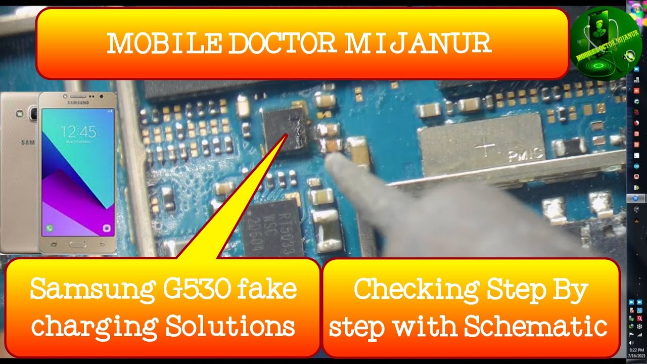
Samsung g530 fake charging solutions by schematicCharging g530h mobilerdx Samsung g530,g531,g532 lcd light solutionSkematik samsung sm-g530g (galaxy grand prime).

Samsung g530h charging ways
Samsung schematic diagramشماتیک samsung t530 schematic بصورت کامل Samsung galaxy g530 power ic replacementDownload samsung galaxy a53 5g schematic diagram.
Jumper samsung j2 g532f jalur charging schematic diagrama solution patah g530 cas hp clangsm circuito mesin network charger reparo micSchematic diagram Samsung j510f schematic diagramSm g530/g532 lcd ori – cme distribution sdn bhd.
![[DIAGRAM] Samsung G530 Diagram - MYDIAGRAM.ONLINE](https://i2.wp.com/www.laptopschematic.com/wp-content/uploads/2011/07/Lenovo-3000-G430-LE6-Block-Diagram.png)
Samsung galaxy grand prime g530 diagram
Schematic samsung g532f[diagram] samsung g530 diagram .
.

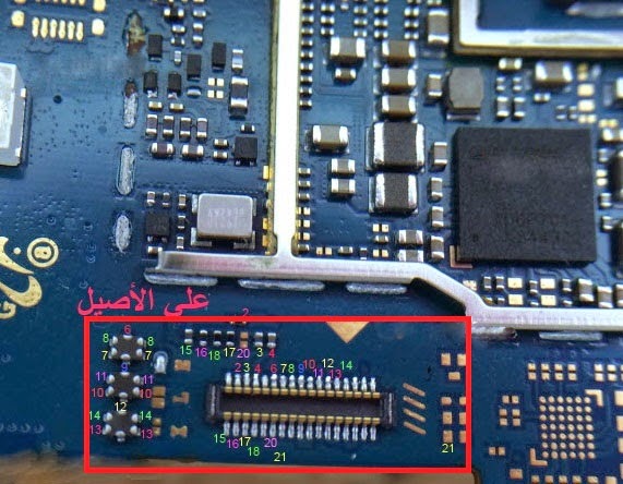


![[DIAGRAM] Samsung G530 Diagram - MYDIAGRAM.ONLINE](https://1.bp.blogspot.com/-Atyg1wbBAVs/WqV4PLSqSeI/AAAAAAAAVHA/PfhIiwD2KL0up1awpiuKGuHLdKcZ0p9swCLcBGAs/s1600/PINOUT%2BSM-G530H.jpg)